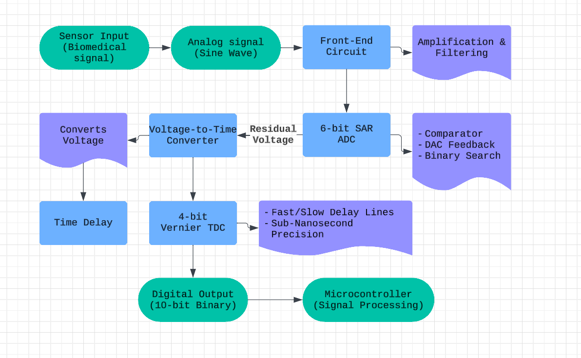
Low-Power Two-Step Successive Approximation ADC
This project develops a low-power 10-bit SAR ADC using a hybrid architecture consisting of a 6-bit voltage-mode SAR ADC, a Voltage-to-Time Converter (VTC), and a 4-bit Vernier Time-to-Digital Converter (TDC). Designed for applications in wireless sensors and biomedical instruments, it emphasizes high efficiency and low power consumption.